

What Is Meant By Load Register From Inputs
Digital Registers
Flip-bomb is a ane chip retentivity cell which tin can exist used for storing the digital data. To increase the storage capacity in terms of number of $.25, nosotros accept to use a grouping of flip-flop. Such a group of flip-flop is known as a Register. The northward-bit annals will consist of due north number of flip-flop and information technology is capable of storing an n-bit discussion.
The binary data in a register can be moved within the register from 1 flip-bomb to some other. The registers that let such data transfers are called equally shift registers. There are iv way of operations of a shift annals.
- Series Input Serial Output
- Serial Input Parallel Output
- Parallel Input Serial Output
- Parallel Input Parallel Output
Serial Input Serial Output
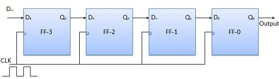
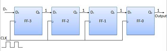
Let all the flip-flop exist initially in the reset condition i.e. Q3 = Q2 = Qi = Q0 = 0. If an entry of a four fleck binary number i 1 1 1 is fabricated into the register, this number should be applied to Din chip with the LSB bit applied first. The D input of FF-3 i.eastward. D3 is connected to serial data input Din . Output of FF-3 i.eastward. Q3 is connected to the input of the side by side flip-bomb i.east. D2 and so on.
Block Diagram
Performance
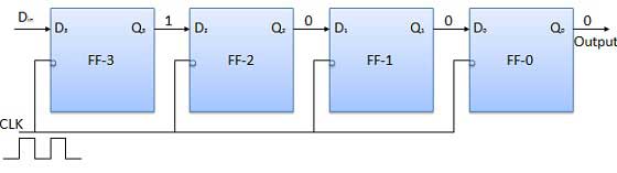
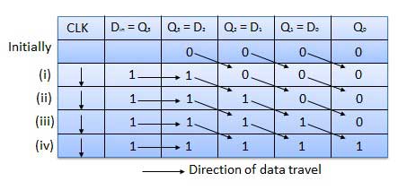
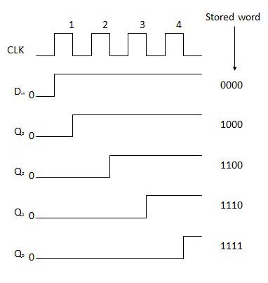
Before application of clock point, let Q3 Qii Q1 Q0 = 0000 and employ LSB bit of the number to be entered to Din. And so Din = Dthree = 1. Utilise the clock. On the starting time falling border of clock, the FF-three is set, and stored word in the register is Q3 Q2 Q1 Q0 = grand.
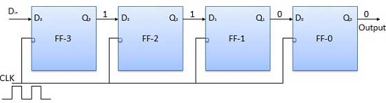
Apply the adjacent bit to Din. And then Din = 1. As before long equally the side by side negative edge of the clock hits, FF-2 will fix and the stored give-and-take change to Qthree Qtwo Q1 Q0 = 1100.
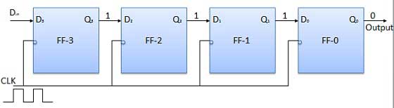
Utilise the next bit to exist stored i.eastward. 1 to Din. Apply the clock pulse. Equally before long as the 3rd negative clock edge hits, FF-ane will be set and output volition be modified to Q3 Q2 Qone Q0 = 1110.
Similarly with Din = 1 and with the fourth negative clock edge arriving, the stored word in the annals is Q3 Qtwo Qi Q0 = 1111.
Truth Tabular array
Waveforms
Serial Input Parallel Output
-
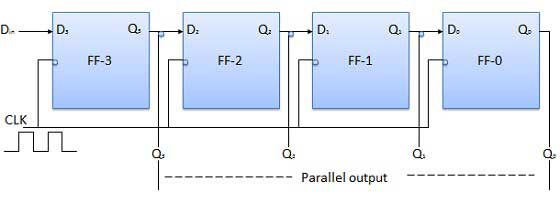
In such types of operations, the data is entered serially and taken out in parallel fashion.
-
Data is loaded scrap by flake. The outputs are disabled equally long equally the data is loading.
-
As presently as the data loading gets completed, all the flip-flops contain their required data, the outputs are enabled and then that all the loaded information is made available over all the output lines at the aforementioned time.
-
iv clock cycles are required to load a four bit word. Hence the speed of functioning of SIPO mode is aforementioned as that of SISO mode.
Block Diagram
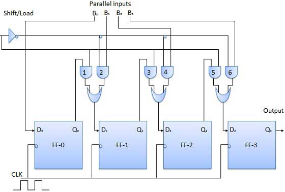
Parallel Input Serial Output (PISO)
-
Data bits are entered in parallel fashion.
-
The excursion shown below is a four chip parallel input serial output register.
-
Output of previous Flip Bomb is connected to the input of the next one via a combinational excursion.
-
The binary input word B0, B1, B2, B3 is applied though the same combinational circuit.
-
There are two modes in which this circuit can work namely - shift mode or load fashion.
Load mode
When the shift/load bar line is depression (0), the AND gate 2, 4 and six go active they will pass B1, B2, B3 $.25 to the corresponding flip-flops. On the low going edge of clock, the binary input B0, B1, B2, B3 will become loaded into the corresponding flip-flops. Thus parallel loading takes place.
Shift mode
When the shift/load bar line is low (1), the AND gate 2, four and 6 become inactive. Hence the parallel loading of the information becomes impossible. Just the AND gate one,three and 5 go active. Therefore the shifting of data from left to right chip by fleck on application of clock pulses. Thus the parallel in serial out performance takes place.
Block Diagram
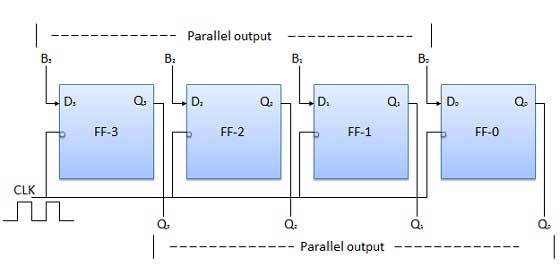
Parallel Input Parallel Output (PIPO)
In this style, the iv scrap binary input B0, B1, B2, B3 is applied to the data inputs D0, D1, Dtwo, D3 respectively of the iv flip-flops. As soon as a negative clock border is applied, the input binary bits volition be loaded into the flip-flops simultaneously. The loaded $.25 will appear simultaneously to the output side. Only clock pulse is essential to load all the bits.
Block Diagram
Bidirectional Shift Register
-
If a binary number is shifted left by one position then it is equivalent to multiplying the original number by ii. Similarly if a binary number is shifted right by one position then information technology is equivalent to dividing the original number by 2.
-
Hence if we want to apply the shift annals to multiply and divide the given binary number, then we should be able to move the information in either left or correct direction.
-
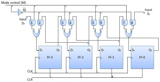
Such a annals is called bi-directional register. A 4 bit bi-directional shift register is shown in fig.
-
There are 2 series inputs namely the series right shift data input DR, and the series left shift data input DL along with a mode select input (M).
Block Diagram
Performance
| S.N. | Status | Operation |
|---|---|---|
| 1 | With Yard = ane − Shift right operation | If M = i, then the AND gates 1, 3, five and 7 are enabled whereas the remaining AND gates two, 4, six and 8 will be disabled. The information at DR is shifted to correct flake by fleck from FF-three to FF-0 on the awarding of clock pulses. Thus with Thousand = one we become the serial right shift operation. |
| 2 | With M = 0 − Shift left operation | When the mode control Thou is connected to 0 then the AND gates two, 4, 6 and eight are enabled while 1, iii, v and vii are disabled. The data at DL is shifted left bit by flake from FF-0 to FF-three on the application of clock pulses. Thus with Grand = 0 we become the serial right shift operation. |
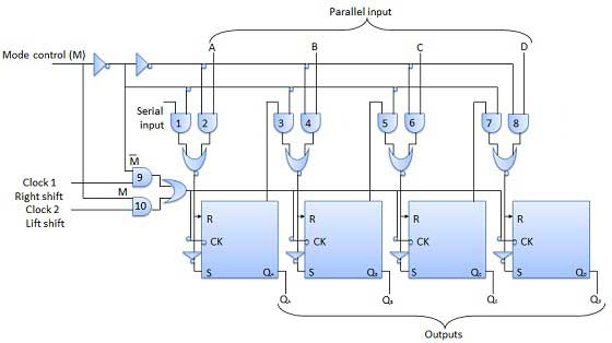
Universal Shift Register
A shift register which can shift the information in only i management is chosen a uni-directional shift register. A shift register which tin shift the data in both directions is called a bi-directional shift register. Applying the same logic, a shift register which tin shift the information in both directions as well as load it parallely, is known as a universal shift register. The shift register is capable of performing the following operation −
- Parallel loading
- Left Shifting
- Right shifting
The mode command input is connected to logic ane for parallel loading performance whereas it is connected to 0 for serial shifting. With mode control pin connected to footing, the universal shift register acts as a bi-directional register. For series left operation, the input is practical to the serial input which goes to AND gate-1 shown in figure. Whereas for the shift right functioning, the series input is applied to D input.
Block Diagram

What Is Meant By Load Register From Inputs,
Source: https://www.tutorialspoint.com/computer_logical_organization/digital_registers.htm
Posted by: linseycathad.blogspot.com
0 Response to "What Is Meant By Load Register From Inputs"
Post a Comment